SN64BCT306
description
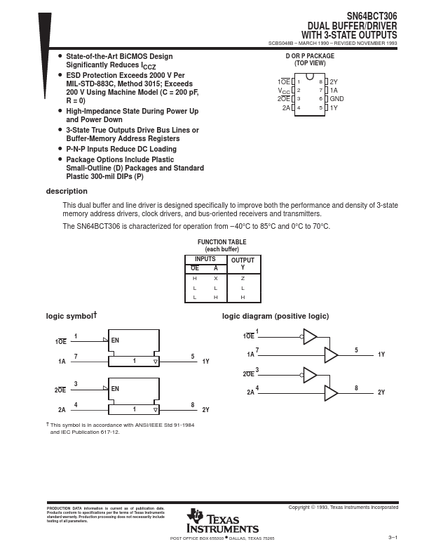
This dual buffer and line driver is designed specifically to improve both the performance and density of 3-state memory address drivers, clock drivers, and bus-oriented receivers and transmitters.
The SN64BCT306 is characterized for operation from
- 40°C to 85°C and 0°C to 70°C.
FUNCTION TABLE (each buffer)
INPUTS OE A
OUTPUT Y
H logic symbol† logic diagram (positive logic)
1 1OE
7 1A
EN 1
5 1Y
3 2OE
48 2A 1 2Y
† This symbol is in accordance with ANSI/IEEE Std 91-1984 and IEC Publication 617-12.
1 1OE
7 1A
3 2OE
4 2A
5 1Y
8 2Y
PRODUCTION DATA information is current as of publication date. Products conform to specifications per the terms of Texas Instruments standard warranty. Production processing does not necessarily include testing of all parameters.
- POST OFFICE BOX 655303 DALLAS, TEXAS 75265
Copyright © 1993, Texas Instruments Incorporated 3- 1
SN64BCT306 DUAL BUFFER/DRIVER WITH 3-STATE OUTPUTS
SCBS048B
- MARCH 1990
- REVISED...